
















Lithography Data Transfer: How 2×100G Fiber NICs with RDMA Keep Mask Data Flowing
In semiconductor manufacturing, the lithography machine writes circuit patterns onto wafers — but on
Read More →
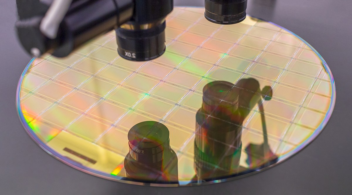


Four purpose-built solutions for semiconductor manufacturing — lithography data transfer, wafer inspection GigE and USB camera capture, and IC packaging & testing. Frame grabber and data transfer NICs from 1G to 200G, frame-loss-free with RDMA.
From wafer fabrication to packaging and testing — data transfer and vision inspection for the entire semiconductor production line
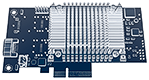
2×100G fiber NIC + RDMA builds a high-speed channel for mask layout data to the lithography machine, ensuring precise pattern transfer to the wafer with low latency.
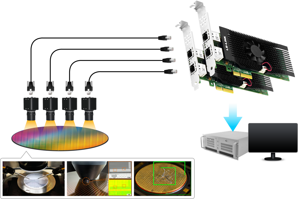
High Speed · Fiber · RDMAFrame grabber cards connect directly to GigE cameras. Jumbo frame + RDMA deliver frame-loss-free wafer defect and critical dimension inspection.
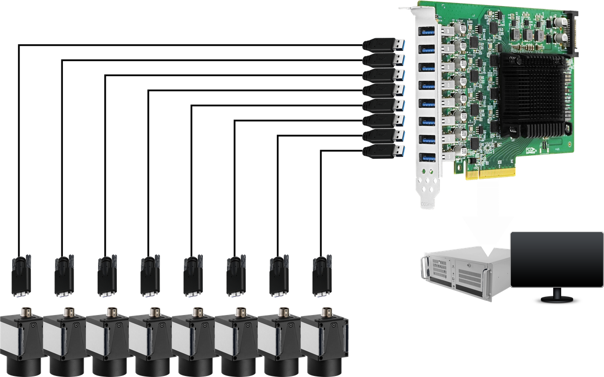
Frame-Loss-Free · With LR-LINKUSB frame grabber cards with multi-port independent bandwidth: plug-and-play, best total cost of ownership, cameras never contend with each other.
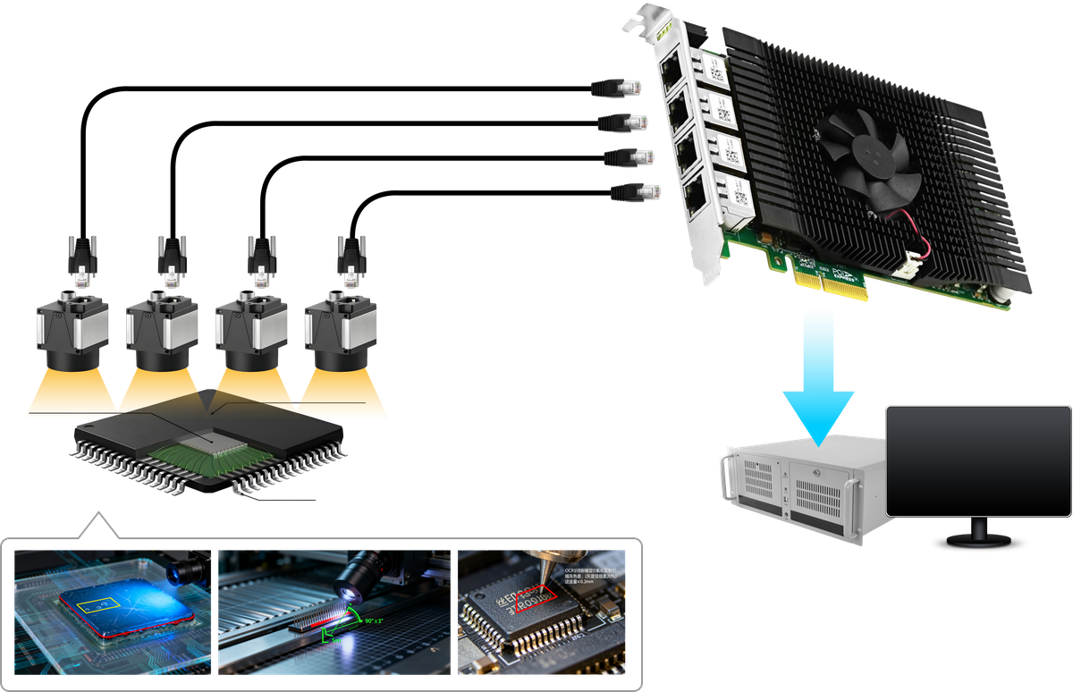
Independent Bandwidth · ReliableVision positioning and defect inspection for wafer dicing, die attach, wire bonding and final test. Gigabit rates, multi-port expansion, simple cabling.
Gigabit-Based · Multi-Port
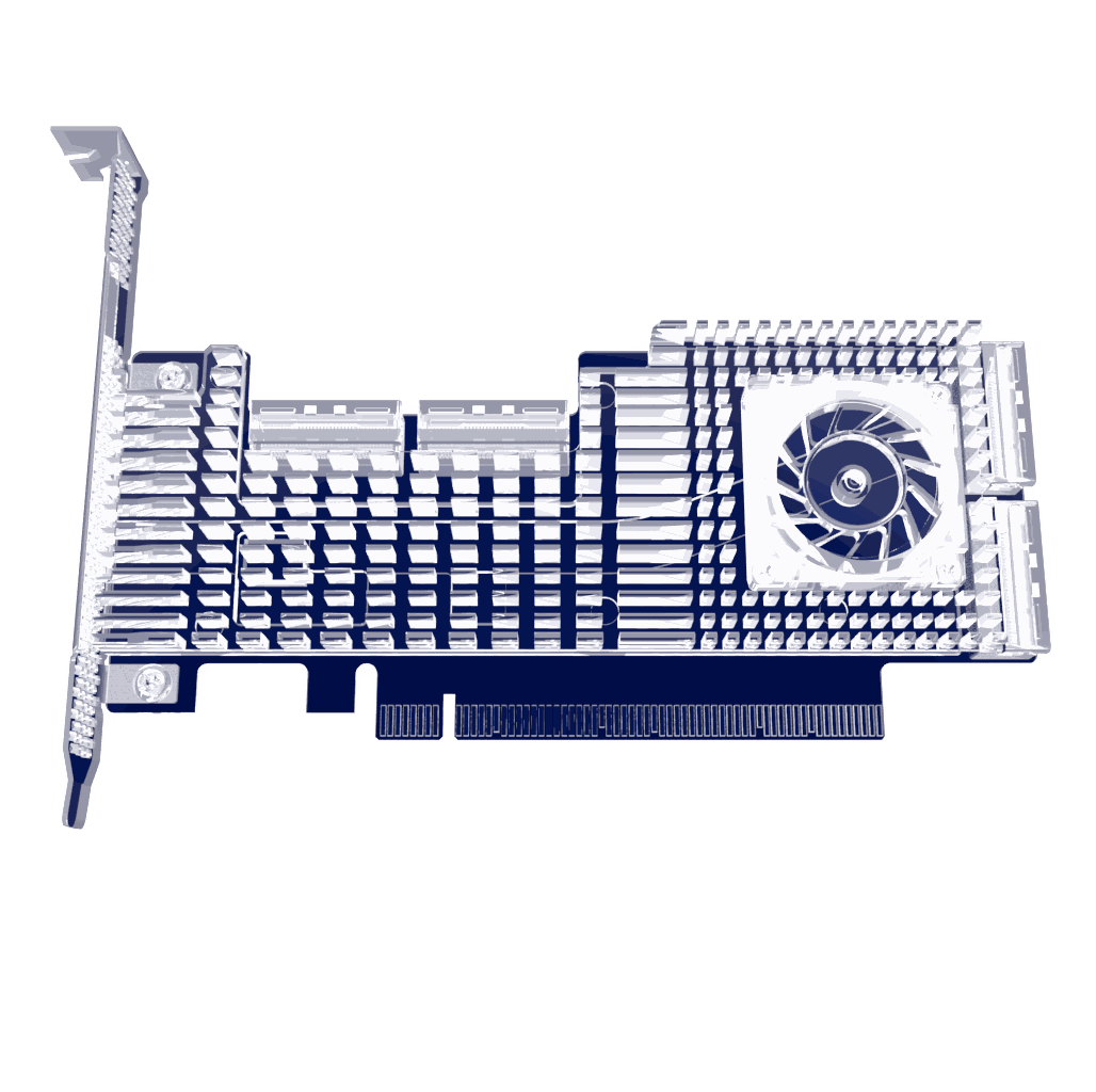
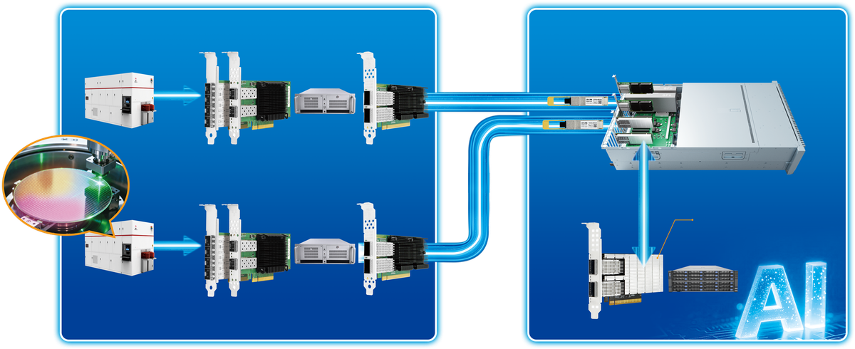
In lithography, mask layout data must travel at high speed between the lithography machine, storage servers and AI servers. A 2×100G fiber NIC with RDMA technology builds a high-reliability, ultra-stable data transfer system.
The NIC provides a high-speed channel for mask layout data to the lithography machine, ensuring precise pattern transfer to the wafer with lower latency.
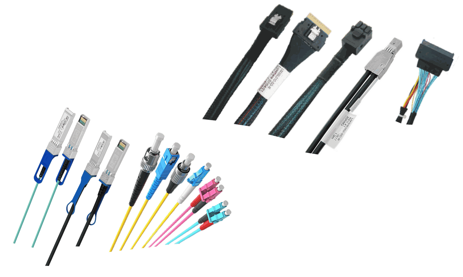
High rates, fiber interfaces and RDMA; the NIC connects FPGA boards or switches.
Covers 25G / 100G / 200G fiber tiers (Intel E810 and more), RDMA supported. Click a model for details.
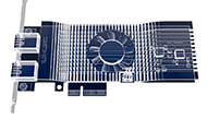
Frame grabber cards connect directly to GigE cameras. Jumbo frame and RDMA features, compatible with mainstream industrial cameras and software, deliver short development cycles and frame-loss-free wafer defect and critical dimension measurement.
Wafer defect and critical dimension measurement with zero frame loss; the NIC connects directly to GigE cameras — shortest link, fewest failure points.
Jumbo frame, RDMA, stability and reliability; NIC connects directly to GigE cameras. Speeds from 1G/2.5G/5G to 10G can be matched to balance bandwidth and cost.
Tiers from 1G / 2.5G / 5G to 10G (quad/1G dual-port PoE in production). RDMA frame grabbers in development. Click a model for details.
USB frame grabber cards connect directly to USB cameras. Multi-port independent bandwidth means cameras never contend; cameras and accessories are easy to source at controlled cost; no complex network configuration — true plug-and-play.
Wafer defect and critical dimension measurement with zero frame loss; best total cost of ownership for concentrated, multi-camera workstations.
Short transmission distance, multi-port, independent bandwidth; NIC connects directly to USB cameras with best total cost of ownership.
USB frame grabbers (5G/10G/20G tiers) are being released progressively; this page will be updated as products launch.
Covers vision positioning and defect inspection for wafer dicing, die attach, wire bonding and final test. Gigabit-rate speeds, multi-port expansion, simple cabling and high stability deliver flexible deployment.
Vision positioning and defect inspection across wafer dicing, die attach, wire bonding and final test.
Gigabit-rate speeds, multi-port expansion, simple cabling and high stability; ideal for detecting broken, sagging or bridged bonding wires, and chip contamination, scratches and edge chipping.
Tiers from 1G / 2.5G / 5G with multi-port expansion and simple cabling (domestic 1G quad-port PoE in production). Click a model for details.
Full range of frame capture and data transfer cards — select by process requirement
| Category | Rate | Frame Capture | Data Transfer | Official Product | |
|---|---|---|---|---|---|
| RJ45 Copper | USB | ||||
| Frame Capture | 1G | 1/2/4/6/8×RJ45 (Intel I350 / I210)In Production1/2/4/8×RJ45 PoE (Intel I350 / I210)In Production4×M12 PoE (Intel I350)In Production | — | — | LRES2049PT-POE (quad-port PoE, domestic)LRES2054PT-POE (dual-port PoE+) |
| 2.5G | 1/4×RJ45 (Intel I225 / I226 / RTL8125)In Production4×RJ45 PoE (Intel I226)In Production | — | — | LRES2058PT-POE (2.5G PoE) | |
| 5G | 4×RJ45 / 4×RJ45 PoE (AQC114)In Production4×RJ45 PoE (RTL8126 / AQC111)In Production | USB 3.0 5Gbps: 2-port USB-C, 4/8-port USB-A (Renesas)In Production | — | LRES2680PT-POE (5G PoE)LRSU9A72-2C (2-port USB-C)LRSU9A71-4A (4-port USB-A)LRSU9A72-8A (8-port USB-A) | |
| 10G | 1/4×RJ45 (AQC113)In Production2×RJ45 (AQC107)In Production4×RJ45 / 4×RJ45 PoEIn Production4×RJ45 (XILINX FPGA)In Production2×RJ45 / 2×RJ45 PoE (AQC113)In Production | USB 3.1 10Gbps: 2/4-port USB-A, dual-port USB-A+CIn Production | — | LRES1013PT (10G quad-port)LRSU3A42-2A (2-port USB-A)LRSU3A42-4A (4-port USB-A)LRSU9A42-AC (2-port: 1×USB-A + 1×USB-C) | |
| 20G | — | 8-channel 8-port 3U (Renesas)In Development8-channel 8-port (ASMedia)In Development | — | 20G USB frame grabber — In Development | |
| USB frame grabbers: 5G tiers (2/4/8-port), 10G tiers (2/4-port) in production — 20G tiers in development. Register via the form for release notification; official links appear above as models go live. | |||||
| Data Transfer | 10G–200G Fiber | Dual-port 25G / 100G / 200G (imported controllers)In ProductionDual-port 25G / 100G / 200G (Broadcom)In ProductionDual/10G quad-port (Intel 700 series)In ProductionDual/25G quad-port, 100G dual-port (Intel E810 series)In Production | — | — | LRES1021PF-2SFP28 (25G dual-port E810)LRES1046PF-2QSFP28 (100G dual-port RDMA)LRES1160PF-2QSFP56 (200G dual-port RDMA) |
Note: Products in development follow official release announcements. For end-of-life products, please consult us for replacement options.
In-depth guides written for this topic — process scenarios, product tiers and selection criteria
In semiconductor manufacturing, the lithography machine writes circuit patterns onto wafers — but on
Read More →
Wafer defect detection and critical dimension measurement run on machine vision — and every dropped
Read More →
When wafer inspection workstations are concentrated and camera counts are high, USB frame grabber ca
Read More →
From wafer dicing to die attach, wire bonding and final test, IC packaging & testing runs on vision
Read More →Full-service support from requirements to after-sales
Clarify process scenario, camera models and bandwidth needs
Match rate tiers and port configurations to the scenario
Validate jumbo frame, RDMA and multi-camera concurrency on real hardware
Multi-tier stocking on demand to keep production lines running
Dedicated NIC solution provider with ongoing technical support
Professional NIC solution provider covering every semiconductor process scenario
From lithography data transfer and wafer inspection to IC packaging & testing — networking and frame capture solutions for the entire semiconductor manufacturing flow.
1G to 200G with copper / USB / fiber form factors — balance bandwidth and cost flexibly; there is always a tier that fits your process.
Compatible with mainstream industrial cameras and software with short development cycles; jumbo frame, RDMA and multi-port independent bandwidth guarantee frame-loss-free inspection.
Ready to get started? Tell us about your semiconductor networking needs — our team will design the right solution for your process.


